Project: lc3-hw [3]: Overall system design
06 Jul 2018
This post is a copy from my old website and blog. I have kept its original post date.
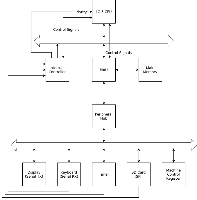
In wake of restricting the scope of the CPU to being what was wrapped by the bus in the previous post, I decided to look at the overall LC-3 system and how to implement it. I settled on having a memory controller and interrupt controller that existed outside of the CPU but still hooked up to the bus and had wires to communicated the control signals to make it compatible with the reference specification of control signals.
To deal with the possibility of new devices, I’ve decided to design and implement an interrupt controller module to handle the now multiple sources of interrupts. This will also integrate into the already specified control signals for interrupts like LD.Vector and GateVector.
Since I had planned on adding more devices besides the already specified keyboard, display, and machine control register the logic to decode and handle memory-mapped I/O would become more and more complex at the level of the memory controller. Thus, I decided to coin what I had called the “memory controller” above as a “Memory Abstraction Unit” (MAU) that presented the MAR/MDR/bus interface with control signals to the CPU, but the underlying “concrete” connections were abstracted away from the CPU and without the CPU knowing about it or caring. While in principle similar to how these memory blocks on the C.8 figure presented themselves to the CPU, I’ve radically changed up the logic besides that of the MAR/MDR/bus interface.
To deal with the growing number of peripherals, I decided that the control signal approach in Appendix C would not scale well. Instead, I opted for a peripheral hub that would communicated with all the devices via a bus (let’s call it the “peripheral bus”) and then communicated with the MAU. Thus, the MAU will decide to communicated with Main Memory or the peripheral Hub depending on if the address in the MAR is in the MMIO (memory-mapped I/O) address space or not.
Here’s the current overall block diagram of my planned LC-3 (with the reference Patt CPU) and the currently planned peripherals:
After I had laid this all out, I realized that I somewhat re-derived the notion of a chipset with a northbridge and a southbridge…
